Working on mechatronics projects involves a fair bit of working with electronics. Prototyping with a breadboard is great for a quick proof of concept. But if the electronic design goes beyond a few components, the amount of wires can become too much to handle. To make things easier, once a segment of the circuit has been tested on a breadboard it is better to move it to a prototype board or a veroboard. A veroboard makes the breadboard circuit more permanent and easy to work with by removing or reducing the amount of jumpers. But you still have to make connections by either soldering jumper wires or making solder traces. And since veroboards are usually single sided, the amount of jumpers are still high. So once a circuit design has been finalised, the best approach is to design and manufacture a printed circuit board (PCB).
Prior to this machine we were using the photolithography and chemical etching method to make PCBs for our projects. This method involves using ultraviolet light to transfer the circuit design onto a copper pcb treated with a photoresist. This cures the photoresist in places where the UV light hits i.e where the circuit traces are. This pcb is then washed in a developing solution which removes the uncured photoresist away leaving behind only the photoresist in places where the traces are. This copper pcb is then placed in a bath of ferric chloride which etches away all the copper not protected by the photoresist. After cleanup only the traces of the circuit design are left on the pcb. The pcb is then ready to be populated, soldered and used. This pcb making process is illustrated in Fig.1.
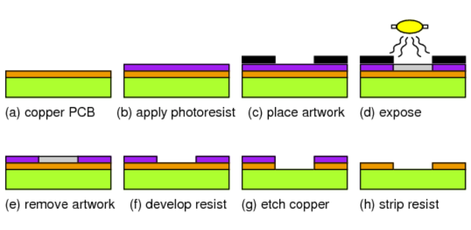
Fig.1
Although this process is great for industrial manufacturing, it is not ideal on a DIY small scale home production. Chemicals used for etching like ferric chloride are unpleasant to work with. Not only does it stain everything that it comes in contact with. It also produces toxic fumes and is corrosive to all metals which means it can’t be simply drained in the sink. It needs proper disposal and safety when using. Working with photoresists is also a finicky business. Exposure and development of the photoresist needs to happen in a dark room because outside light will cause unwanted exposure of the photoresist which will ruin the result. Also timing of the UV exposure needs to be just right. Less exposure time will result in the photoresist being undercured and will partially wash off during the developing stage. Too much exposure time will cause excess unwanted curing of photoresist surrounding the required region. This will cause adjacent traces to merge.
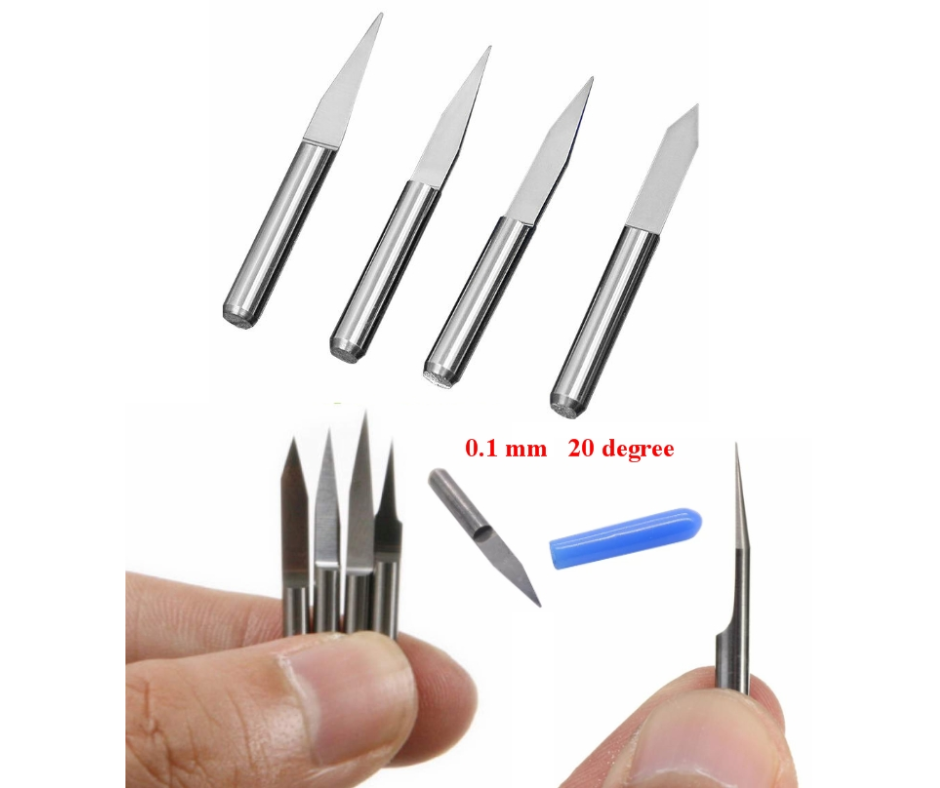
Fig.2
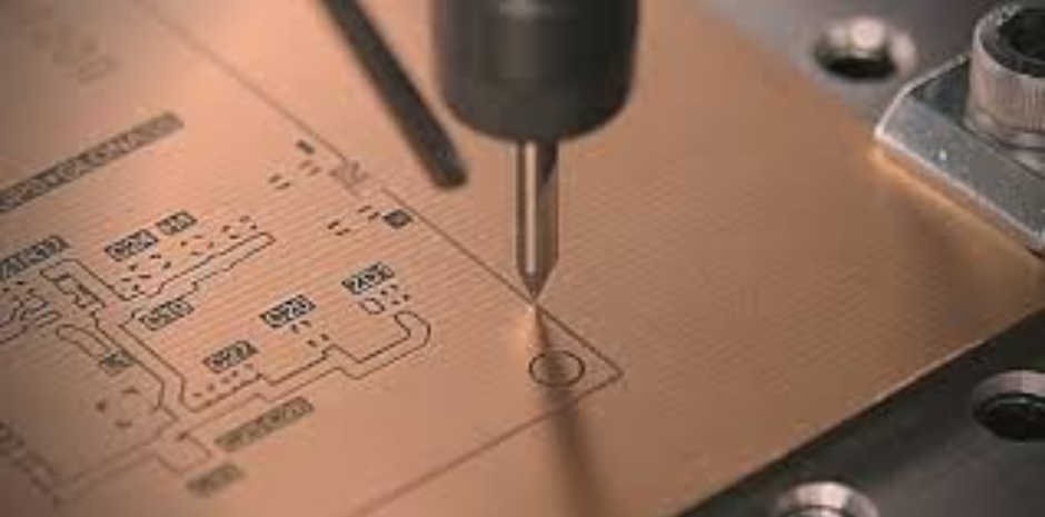
Fig.3
An alternate to the chemical process is the mechanical process which involves using a cnc machine to mechanically remove unwanted copper from the pcb. A very thin ‘V’ shaped bit such as one shown in FIg.2 are used to mechanically form very fine traces for circuits as shown in Fig.3. This mechanical process, although unfeasible for large scale commercial pcb manufacturing, is ideal for DIY pcb manufacturing at home.
There are many commercially available small CNC designs and kits. Many of these small CNC machines follow the same design to the machines shown in Fig.4 and Fig.5.

Fig.4
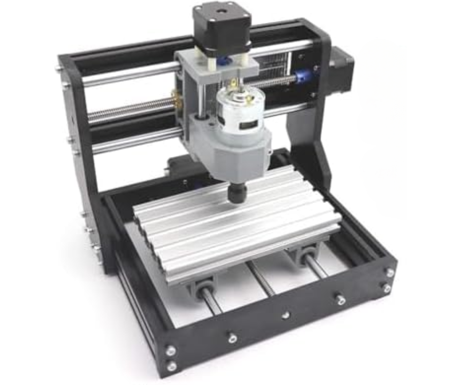
Fig.5
In this design the workbed moves in the Y axis and the toolhead moves in X axis and Z axis. Although this design is great for light cutting and milling, it suffers from issues of rigidity as shown in Fig.6.
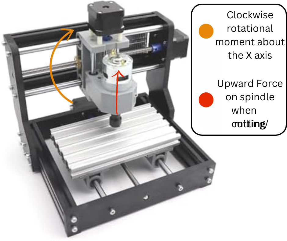
Fig.6
When the toolhead is cutting it is exerting a force down on the workpiece which inturn exerts an upward force on the toolhead. The upward force causes the toolhead to rotate about the X axis. Since the toolhead is mounted on X axis linear rods/rails, the rotation moment causes the toolhead to deflect. The degree of deflection depends on the thickness of the linear rods/rails used and the rigidity of the construction of the cnc body.
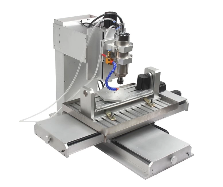
Fig.7
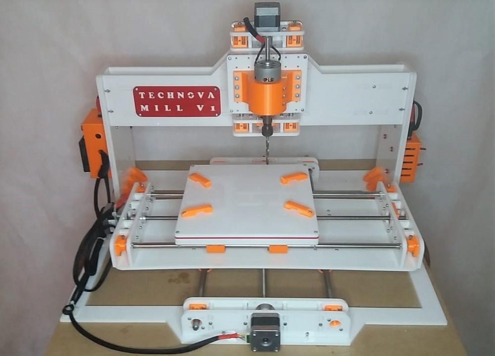
Another design of desktop cnc machines is shown in Fig.7. In this design the workbed moves in both X axis and Y axis. The toolhead only moves in the Z axis. This results in the toolhead to be more rigid since there is no horizontal axis for the toolhead to rotate about. This design is more rigid and accurate when cutting/milling. This is the design type that we adopted for our desktop cnc. When researching this design for use in pcb manufacturing, we came across inspiration in the form of a commercially available pcb manufacturing desktop cnc machine that matched our requirement.
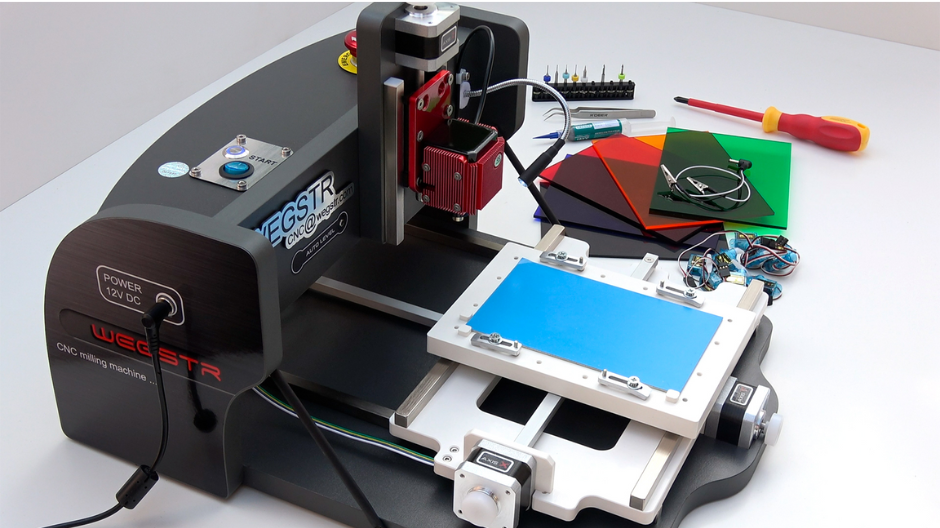
Fig.8
Fig.8 shows a pcb milling machine from wegstr. This machine has all the qualities that we desired in our cnc machine. So we decided to design our cnc machine similar to the wegstr machine.
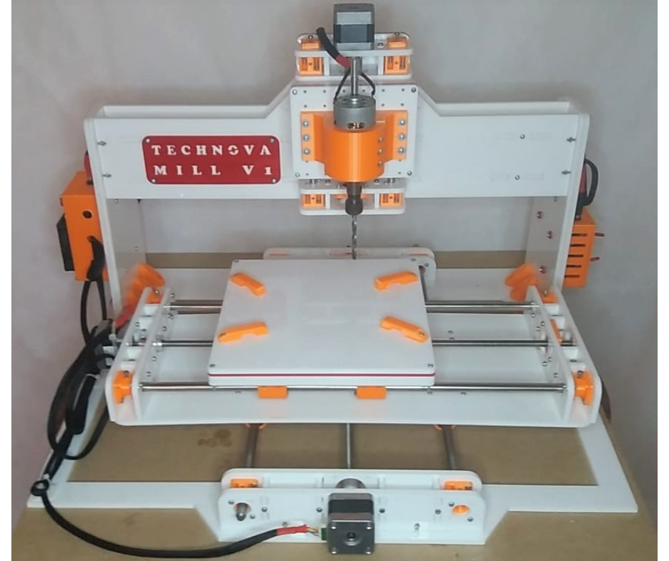
Fig.9
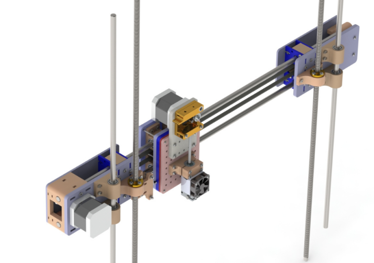
Fig.9 shows the first prototype of our Desktop CNC design. Our design is quite similar to the wegstr machine shown in Fig.8. We have designed our machine to have a working volume of 20cmx20cmx10cm. The workbed has an area of 20cmx20cm. There are some differences in our design that came about due to availability and cost of raw material. In our design we use linear rods and linear ball bearings (Fig.10) in our motion system as an alternate to the linear rails (Fig.10) that are used in the wegstr machine. The main reason for this difference is the cost. In Pakistan where we have developed this machine, the cost difference between linear bearings (with linear rods) and linear rails is more than 6 times. This means that at the cost of equipping just one axis with linear rails, we can equip two entire machines with linear bearings and rods.
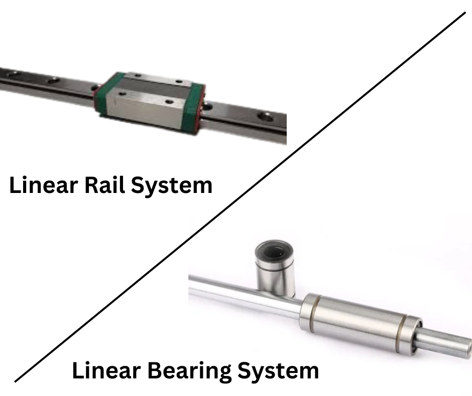
Fig.10
Now linear rails are by design more rigid and stable than linear bearings and rods. But keeping in mind that our machine is designed for machining soft materials and therefore will not experience excessive forces, the use of linear bearings and rods is sufficient. Additionally we have used beefy 10mm stainless steel rods with 10mm linear bearings in our machine.
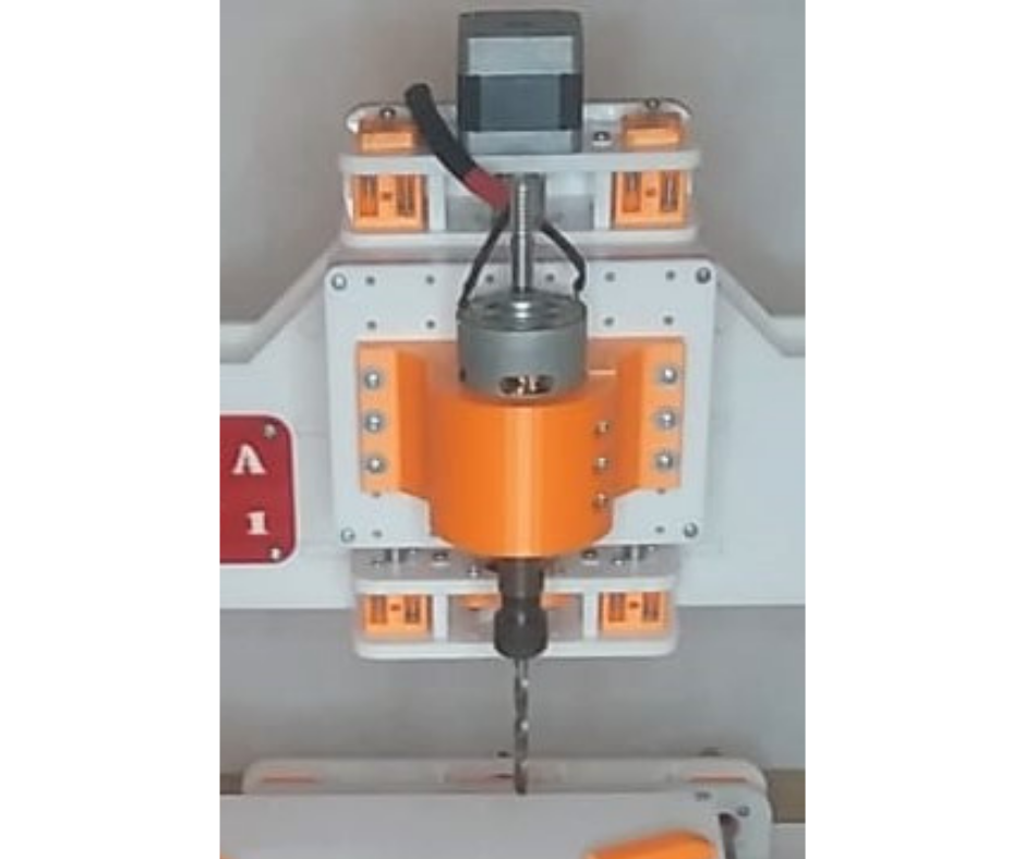
Fig.11
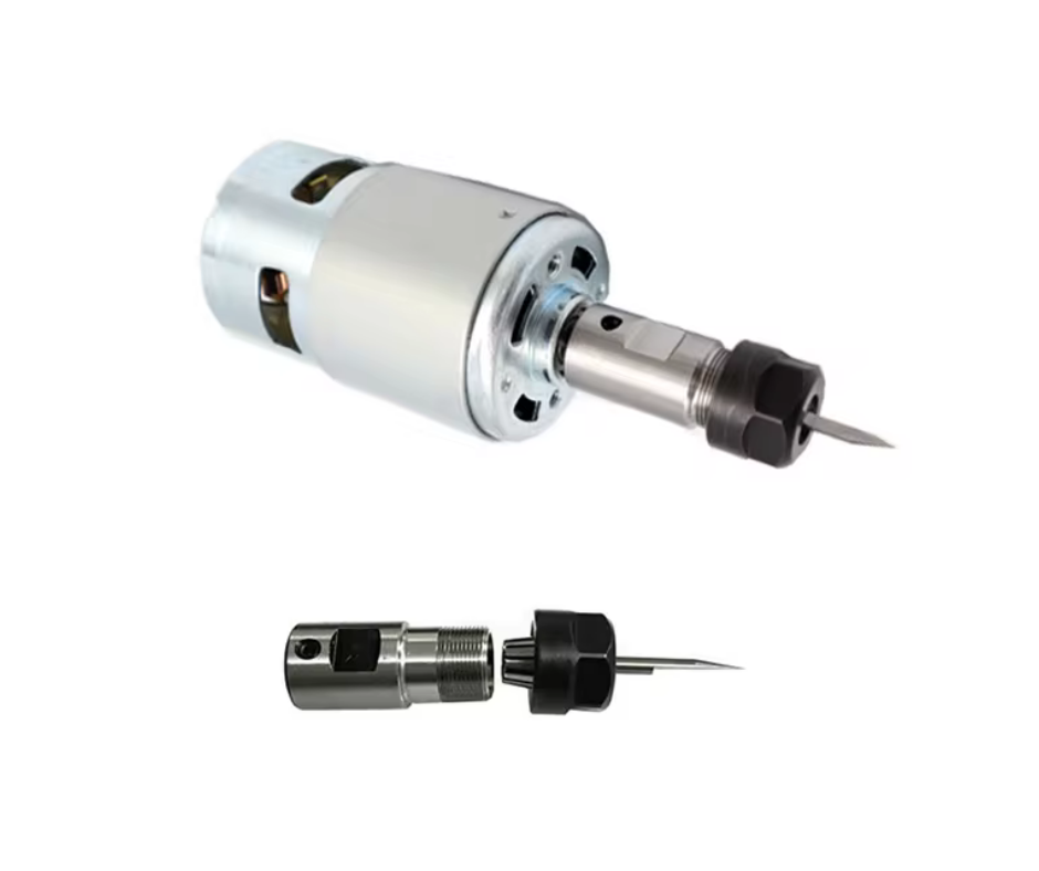
Fig.12
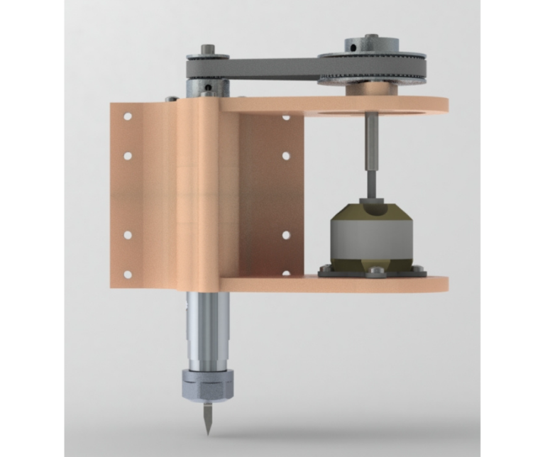
In our machine design the toolhead carriage is rigidly attached to the structure of the machine as shown in Fig.11. The tool (spindle) in the toolhead carriage can move up and down in the Z axis. In our machine we have used a 755 motor with an er11 collet as shown in Fig.12. Since the tool carriage is rigidly attached to the machine structure, it adds rigidity to the tool when being used and prevents rotational moments on the toolhead carriage.
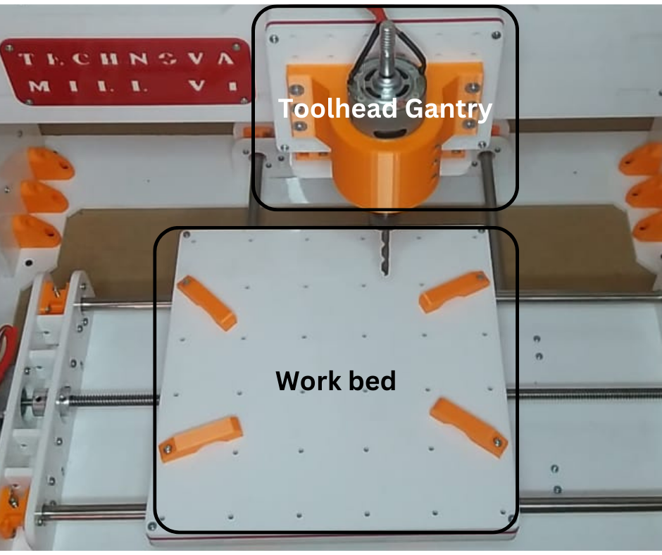
Fig.13
The workbed of our machine as shown in Fig.13 has multiple evenly spaced holes which each contain a captive nut underneath. These holes can be used to attach clamps, workpieces, etc to the workbed. This increases the overall utility of the machine. The same type of attachment mechanism is also employed for the toolhead gantry. This allows different types of tools to be attached to the toolhead gantry. As can be shown in Fig.13 we have attached a spindle as a tool to the toolhead gantry. We can very easily attach any other tool to the toolhead gantry by simply 3D Printing an appropriate mount and attaching it to the toolhead gantry.
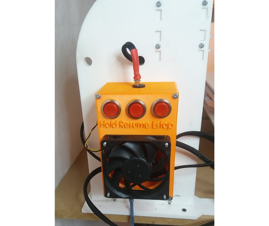
Fig.14
Fig.14 shows the control box of our CNC machine. We use an arduino uno with a GRBL shield as the brains of our machine. The control box also features easy to reach buttons for some essential functions such as emergency stop. Our cnc machine also features auto probing for the purpose of pcb milling. This is an extremely useful feature because it allows the machine to generate a height map for the copper board and then adjust the Z height of the tool to ensure that the cutting depth is maintained and not over or under cutting due to uneven surfaces.
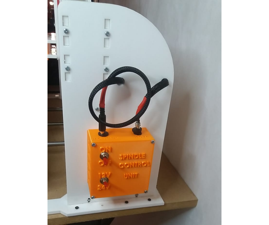
Fig.15
Fig.15 shows the power distribution and spindle control box. This box contains DC to DC convertors to efficiently convert the input voltage into appropriate voltages for both the control electronics and the spindle/tool. We have also left provisions to install a DC speed controller to control the speed of the spindle.
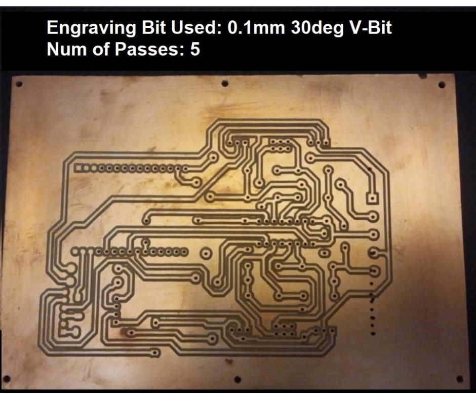
Fig.16
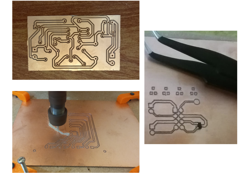
Fig.17
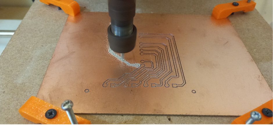
Fig.18
Fig.16 through Fig.21 shows the cutting and engraving capabilities of our cnc machine. Fig.16 Fig.17 and Fig.18 shows the pcb milling capabilities of our cnc machine which is a primary function of our machine. As can be seen from these figures our machine is more than capable of milling very fine traces and pad. Our machine can even mill SMD sizes.
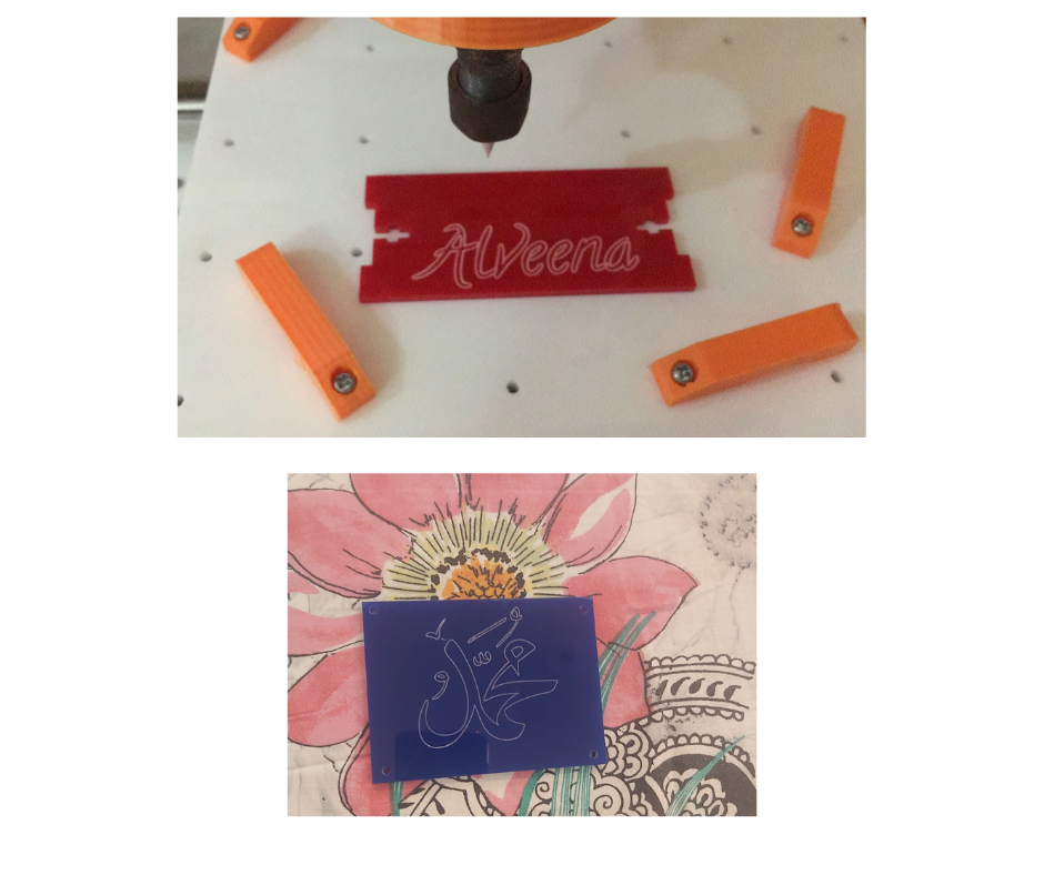
Fig.19
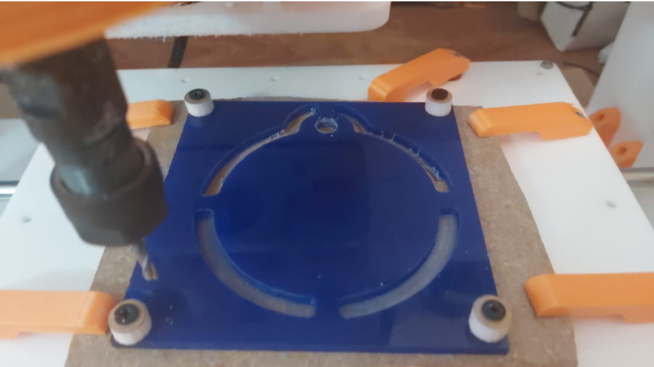
Fig.20
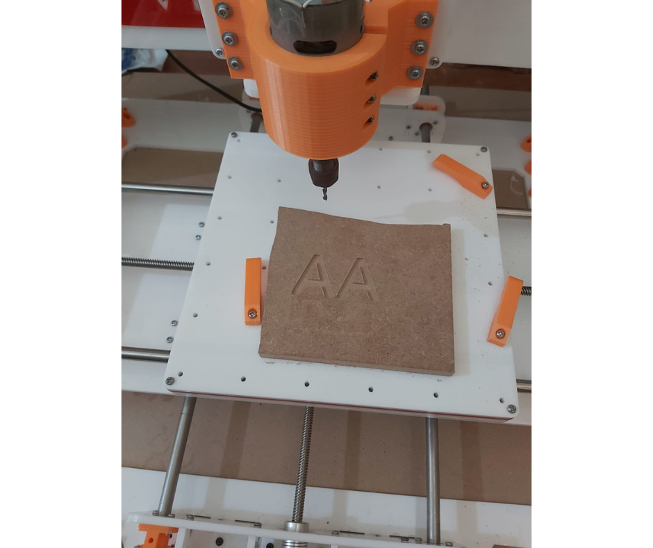
Fig.21
Fig.19 and Fig.20 show the results of cutting and milling acrylic. Fig.21 shows the results of milling MDF board. These results highlight the capabilities of our machine in engraving and milling soft materials such as acrylic and mdf. This shows that our cnc machine in addition to pcb milling can also be used for a myriad of different applications as well.
We will be continuing to work on improving this design as we get more feedback from using the machine. Stay tuned for more updates and upgrades.